DBNZ CPU
I’ve decided to build a CPU that supports only one instruction: DBNZ. That
is, Decrement and Branch if Not Zero. Each instruction consists of two bytes.
The first gives a memory location whose value should be decremented, and the
second consists of the memory location from which to fetch the next instruction
if the result is non-zero. Using only this instruction and some self-modifying
code cleverness, you can write a surprising number of programs.
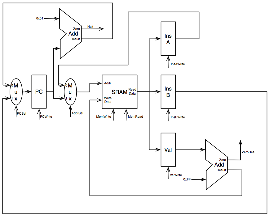
Following examples I saw in Computer Organization and Design, I’ve sketched out a data path for the CPU:

Some relevant pieces (all registers, adders, and buses are 8 bits wide):
-
PCis a register that contains the address of the instruction to be fetched. It can be set from the +1 adder (for incrementing), or fromIns B(for branches). The +1 adder is set up to raise aHaltsignal that will halt the external clock circuitry when the CPU jumps to0xFF. -
There is an SRAM unit that can be told to store the supplied write data at the given address, or to read the data at the given address. The address is supplied by
PC(for loading instructions) orIns A(for loading values to be decremented). -
Ins Aholds the first byte of the instruction, i.e. the address of the value to be decremented. -
Ins Bholds the second byte of the instruction, i.e. the address to jump to if the result of the decrement is not zero. -
Valholds the value to be decremented, and is set up to send its value from an adder that will do the decrementing. The adder is set up to raise aZeroRessignal when the result of decrementing is zero; this feeds into the control circuitry.
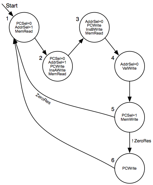
Here’s the control logic:

-
Set up the memory to read from the address in
PC, and preparePCto be incremented. (The value from the adder will be stored on the rising edge ofPCWrite, asserted in the next state.) -
Store the first byte of the instruction into
Ins Aand incrementPC. (Assuming no large clock skew, there’s no race condition here because the hold time required for storing intoIns Ais much lower than the propogation delay ofPC, much less that of the SRAM.) KeepMemReadasserted withAddrSel=1so that the memory outputs the next byte. -
Store the second byte of the instruction into
Ins Band incrementPCagain. Set up the memory to read from the address in the first byte of the instruction. -
Store the value pointed at by
Ins AintoVal. The adder will then output that value minus one. Continue to setAddrSel=0so that this can be written back to the memory. -
Write the decremented value back to memory. Set up
PCto read fromIns Bin case we jump. If the decrementing logic says that the result is zero, fall through to the next instruction in memory by going to state 1. -
Store the jump target into
PC.
I think this can be implemented with a resettable decade counter (actually a count-to-6 chip, if such a thing exists) and a few logic gates. The only thing that remains is a clock generator and a system to load a program into memory and reset the CPU. I’ll probably set up an Atmel MCU to do both of these, reading the program from a Micro SD card.
TODO: Check on some timing issues:
-
Make sure the SRAM’s propogation delay is higher than its address input’s required hold time; otherwise incrementing
PCwhile reading an instruction byte will be unstable. -
Make sure the SRAM’s propogation delay is higher than the register’s hold time plus all of the propogation delays involved in setting register control signals such as
InsAWrite. Otherwise, we won’t load well-defined values into the registers from memory. -
Make sure the mux’s propogation delay is higher than the SRAM’s address hold time requirement; otherwise we won’t have a well-defined address in the transition from state 2 to state 3.
-
Make sure that the propogation delay for turning off
MemReadis greater than the hold time for the registers; otherwise we won’t get a well-defined value inVal. -
Consider having
PCSel=0be defined to continue into state 3,AddrSel=0into state 5, andPCSel=1into state 6, so that the control of the relevant mux is guaranteed not to change near the assertion of the appropriate write signal.